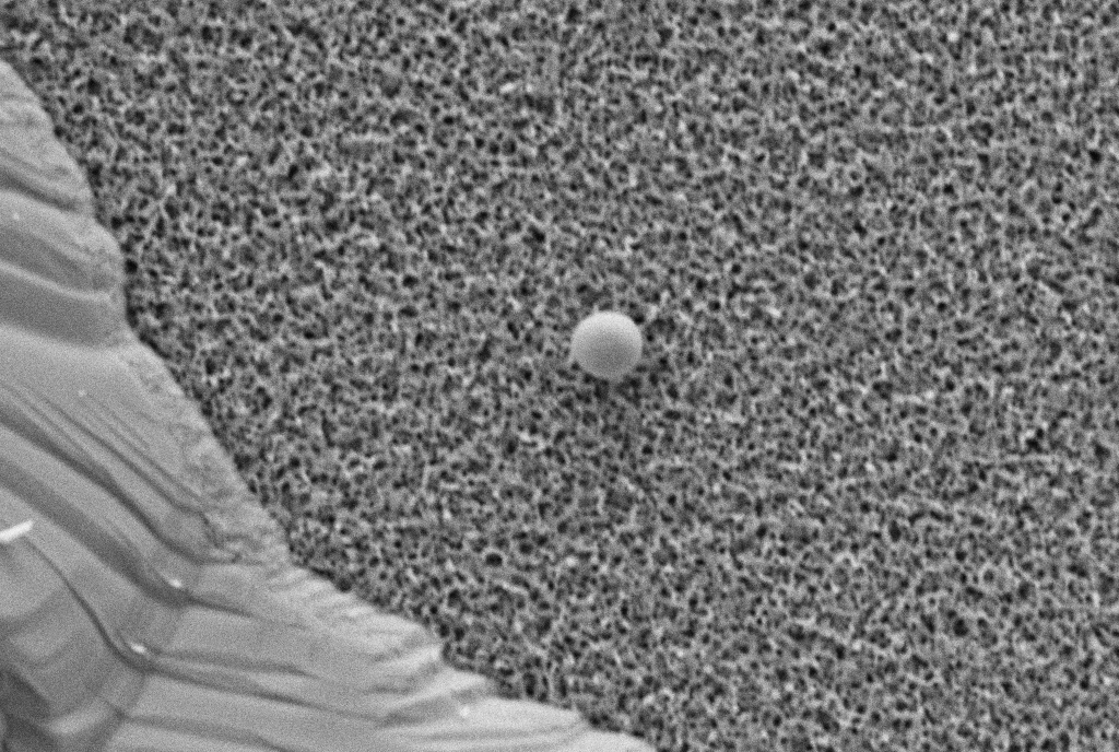
Porous silicon
Electrochemical porous layer formation of silicon is used to condition the silicon wafer surface in such a way as to allow for a detachment of an epitaxially grown silicon wafer. The focus lies on the crystallographic and electrical characterization of the epitaxial silicon layer in dependence of the properties of the porous silicon layer. A classical two chamber etching tool is available for wafer sizes 156 mm x 156 mm and 200 mm round.