Back contact solar cells
Back contact solar cell feature both contact polarities on the rear side of the solar cell. In addition, the pn-junction is also located at the rear. For a lean solar cell fabrication process our group developed an approach based on CVD-doping sources. Besides the electrical properties of the pn-junction (e. g. saturation current) also the generation of defects during junction formation e. g. by laser application is investigated.
Heterojunction and passivating contacts
Silicon solar cells with hetero emitter consisting of an intrinsic and a doped amorphous silicon layer on a crystalline silicon wafer offer highest conversion efficiencies at process temperatures belo 250°C. The amorphous silicon layer at the solar cell front side leads to a significant loss in short circuit current and thus power. Therefore the development focusses on a rear junction or on approaches with less absorbing layers as of SiOx, SiOxNy, SiCx or nc-Si. Due to the low lateral conductivity of the emitter layer despite of high doping a transparent conducting oxide layer as indium tin oxide or aluminum-doped zinc oxide is deposited. For a high conversion efficiency of these hertero junction solar cells an alignment of band bending at the surface and work function of the TCO and contact metal is necessary.
The very high efficiency potential is realized because the contact recombination is significantly reduced. This approach is also applied for the formation of passivating contacts for which an interface oxide is used in combination with a doped amorphous or polycrystalline silicon layer bending the valence and conduction bands of the silicon wafer in a way that leads to charge carrier selective contacts.
Highly doped layers
The doping for the formation of the pn-junction can be carried out by different methods. Conventionally a POCl3 or BBr3 source in combination with a high temperature step at above 800°C is used. Since such a diffusion occurs from the gas phase both sides of a wafer are doped unless a masking layer is deposited. However, dopant sources can also be deposited on just the desired are of a wafer by using inks or paste for printing or CVD as well as PVD. Such layers contain dopant that are subsequently driven into the silicon by high temperature. The ldopant layer can als be used as passivating layers.
Structural properties of doping glasses as well as conductivity and light absorption in dependence of bonding concentrations are investigated.
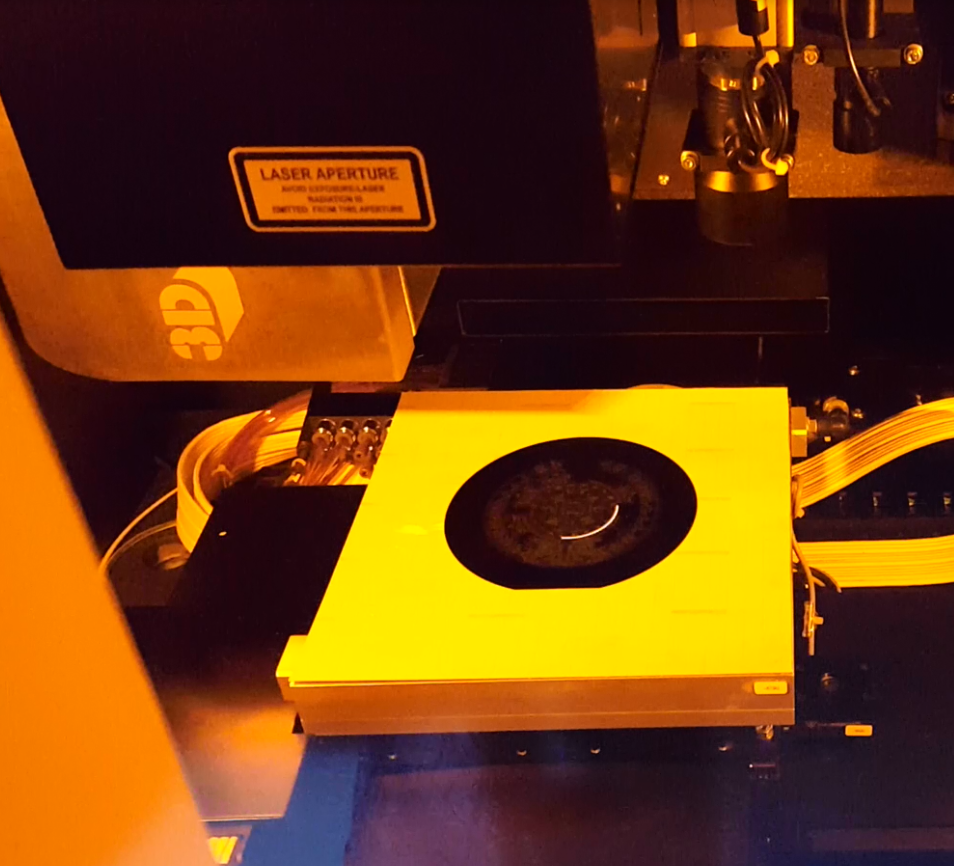
LASER-material interaction
Aiming at a doping of silicon applying nanosecond or picosecond pulse lasers with wavelengths of 355, 532 and 1064 nm we investigate the melting and recrystallization of the silicon wafer surface as well as the activation of dopants in the silicon lattice by laser light.
An additional topic is the dewetting of silicon surfaces or silicon oxide surfaces by laser light using laser interference. Here we collaborate with Johannes Boneberg’s group, for utilizing such processes for the silicon solar cell fabrication.